Powering AI: Semiconductor manufacturing solutions

Artificial intelligence (AI) has advanced rapidly in the last few years, revolutionizing industries and changing the way we go about our day-to-day lives. This unprecedented growth has placed intense computational pressure at the back-end, where larger memory capacities and faster processing speeds are required to handle AI data transactions. A crucial component of this process is high performance semiconductors. The AI semiconductor market is forecasted to reach $159 billion by 2028, more than double the projected $71.3 billion in 2024. To enable chipmakers to build more efficient and powerful chips, the manufacturing technology behind them must also continue to evolve. Hanwha Precision Machinery, a globally renowned advanced manufacturing solutions company, has consistently invested in the research and development of this technology for over 30 years, supplying chip manufacturers around the world with highly specialized machinery.
In this article, we’ll look at some of the challenges that arise from building advanced chips, and how specialized solutions, like those Hanwha Precision Machinery is delivering, can help to overcome them.

AI’s growing need for advanced chips
As AI integrates further into our lives, the need for computational power and efficiency has never been greater. Another semiconductor shortage — like the one faced during the pandemic — could become inevitable, driven by a rising need in data centers to support cloud AI and AI-enabled devices.
The amount of data transactions required to realize AI is much greater than what conventional semiconductor technology can handle. Demand now necessitates a new chip structure capable of processing more data within the same time frame and physical area.
Chips feature transistors — tiny switches that control electrical current flow and power computing functions such as memory and logic. The more transistors a chip has, the more data it can process, and the more advanced it becomes. Over time, chip manufacturing technology has evolved to make each of those transistors as small as possible — nanometer scale, in fact. Because of this, the chip manufacturing process has traditionally focused on the front-end production stage, where transistors are designed and printed. However, chips are reaching their physical limits. Even as engineers work to further reduce overall chip size by reducing the distance between transistors from 3nm to 2nm, traditional 2D chip structure has simply run out of space.
To address this issue, chipmakers have turned to stacking chips vertically, a modern technique that’s also great for improving processing speeds. Processing speed directly depends on the number of transistors connected, and when space runs out, stacking up becomes the solution — but only if the right technology exists to enable communication between layers. That’s where specialized back-end production plays a crucial role.
With advanced packaging technology, transistors can be arranged partially side-by-side (2.5D) or fully stacked (3D), with each layer electronically connected via holes, or completely attached to the transistor’s top and bottom layers. This is possible through processes like thermal compression and hybrid bonding, which support faster processing and cost-efficient production. The future of advanced chip manufacturing now lies in building upward.
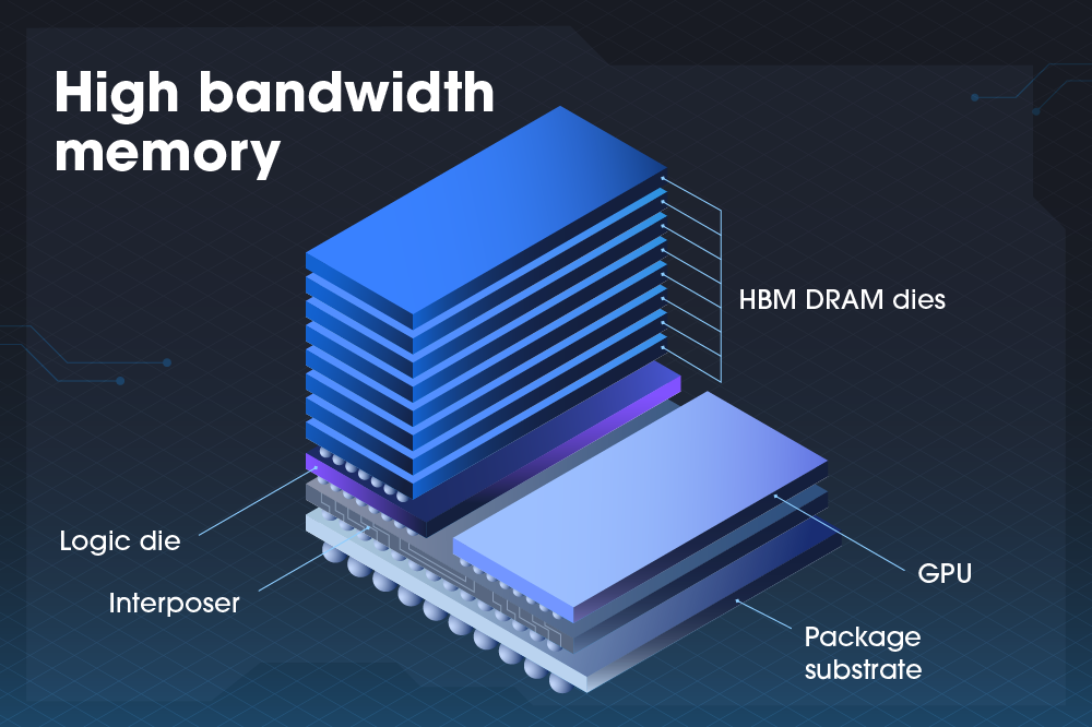
The “stacking-up” method is also used in the manufacture of high bandwidth memory (HBM), a specialized type of memory chip with more capacity than the traditional dynamic random-access memory (DRAM).

What is HBM and why is it important?
HBM is an essential component of the graphics processing units (GPUs) that drive ChatGPT and other generative AI systems. It is capable of transferring data faster than any other memory chip, making it especially well-suited for heavy computational tasks. By vertically stacking layers of the most advanced DRAMs, HBM significantly increases data transfer speeds between the memory and processing units, reduces latency, and delivers larger data bandwidth — crucial for handling hefty AI model throughput.
Since its introduction in 2013, HBM has steadily been evolving. The forthcoming era of HBM4 is poised to propel bandwidth and efficiency to another level. Optimized for data centers, AI, machine learning, and graphics-intensive applications, HBM4 is expected to feature stacks of 16 or more chips, surpassing the 12 layers found in current HBM3 and HBM3E stacks. As the growing need for higher performing memory outpaces production capacity, companies are racing to secure the next generation of advanced packaging solutions to meet demand.
However, manufacturing HBM is expensive: it can cost up to five times more than conventional DRAMs. While HBM supply is expected to grow, with bit shipments projected to reach a compound annual growth rate (CAGR) of 45% in the next five years, the price tag of these chips is expected to remain high. This is due to the intense technical complexity of manufacturing them and the continual outpacing of demand by AI’s computing needs.
So, what exactly does it take to manufacture these advanced semiconductors?

Advanced manufacturing: Supplying solutions for next-generation AI
AI’s rapid growth is not only driving the need for higher performing chips, but also for the advanced manufacturing technology required to build them. Building semiconductors is a highly intricate, delicate process that spans eight key stages: five in the front-end process, where circuits are precisely printed onto wafers, and three in the back-end process, where printed pieces are lifted off, packaged, and rigorously tested. To put this process into perspective, incredibly specialized equipment is required to handle dimensions as small as 10 micrometers — 10 times thinner than a single human hair. The higher performing the chip, the tighter tolerance needed to produce it. Building new chips is time-consuming, too: the journey from initial research and development to mass production can take up to 10 years.
On top of the growing demand driven by new AI applications, the semiconductor industry has traditionally been sensitive to socioeconomic change. In a rapid AI adoption scenario — which anticipates 31% growth in PCs and 15% growth in smartphones — the number of semiconductor fabrication facilities (or fabs, where the AI chips are made) would need to increase by four to raise output by an estimated 25% to 35%. Meanwhile, data centers and servers are estimated to grow faster within the next couple of years due to AI, intensifying the risk of a shortage in chip supply.
To mitigate disruptions to the supply chain and meet explosive demand, a robust response that supports increased semiconductor manufacturing capacity is needed. Companies like Hanwha Precision Machinery are key to ensuring a strong supply chain, providing cutting-edge tools and technologies to global semiconductor manufacturers. With equipment that spans both the front and back-end processes, Hanwha Precision Machinery is able to respond to market changes quickly, bringing the latest in advanced manufacturing equipment to market sooner.

Hanwha Precision Machinery: Innovating the next era
In 1989, Hanwha Precision Machinery started out as the first chip mounting business in Korea. Inspired by the vision and precision technology of the company’s beginnings, Hanwha Precision Machinery began researching and developing semiconductor packaging equipment in 1993. Since then, it has won two innovation awards and become a leading provider in precision tools. Its semiconductor equipment business has primarily been focused on the back-end packaging of building both conventional and advanced chips.
Currently, Hanwha Precision Machinery is developing a revolutionary hybrid bonder to build the technology that’s set to play a “starring role” in the manufacture of advanced 3D chips. Hybrid bonding enables the stacking of chips by reducing the gap between transistor layers and bonding the surfaces of chips together. This process not only significantly decreases the overall thickness of HBM but also dramatically improves data transaction speed between layers, resulting in the highest performing semiconductors to date.
Hanwha Precision Machinery has been working with the world’s leading chipmakers to build and provide next-generation semiconductor manufacturing solutions. Global partnerships such as these cement Hanwha Precision Machinery’s role as a comprehensive semiconductor equipment manufacturer, integrating the company’s state-of-the-art tools for each step of the advanced chip building process. Through these solutions, the company is actively contributing to the robust development and accessibility of higher performance chips, and ensuring the continued evolution of AI.
Get the latest news about Hanwha, right in your inbox.
Fields marked with * are mandatory.
- Non-employee
- Employee


